Specifications
In this section it will be described the electrical characteristics of the OBDH hardware, its connections and physical properties .
Physical Properties
- Operational Temperature: -40° to +80° C
- Dimensions: 92mm x 89mm x Xmm
- Mass: xx.x g
- PCB Material: FR-4
- Layers: 2
Electrical Characteristics
| Parameter |
Condition |
Min |
Typ. |
Max |
Unit |
| Main VCC |
Power source |
3.2 |
3.3 |
3.4 |
V |
| Clock Frequency |
|
1 |
8 |
32 |
MHz |
| Current consumption |
@3.3 V, @32MHz, All tasks |
x |
x |
x |
mA |
| Current Drivers VCC |
Power source |
2.7 |
8.4 |
10.8 |
V |
| Antenna Deployer VCC |
Power source |
3.2 |
3.3 |
3.4 |
V |
Interfaces
The OBDH have a total of 13 connectors:
- 2 for the PC104 interface
- 1 for each solar panel equipped with magnetorquers, a total of 3
- 2 for the Antenna Deployer
- 2 three way jumpers
- 3 for debug purpose
- 1 for the JTAG programming interface
The figure below highlight these connectors.
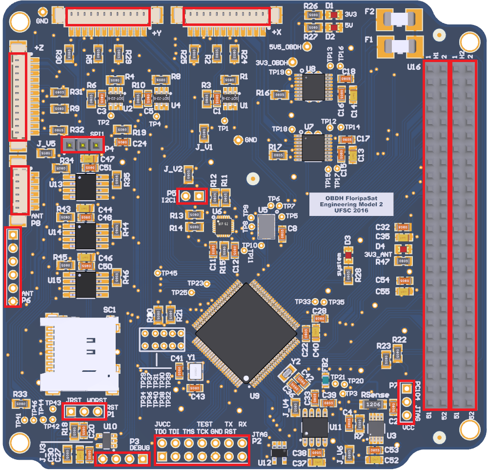
OBDH Connectors
Obdh PC104 interface
The PC104 connects all boards of the cubesat through a single interface. The figure below shows the PC104. Also the tables show the obdh pins

PC104 pins. Internal one(left) and the External one(right).
Internal(H1)
| Number |
NAME |
DESCRIPTION |
| 1 |
GND |
Ground |
| 2 |
GND |
Ground |
| 3 |
GND |
Ground |
| 4 |
GND |
Ground |
| 5 |
TTC_CTRL_RF_SWT_RX |
Radio Control switch TX |
| 6 |
TTC_CTRL_RF_SWT_TX |
Radio Control switch RX |
| 7 |
TTC_GPIO0_MAIN |
Main Radio GPIO 0 |
| 8 |
TTC_GPIO1_MAIN |
Main Radio GPIO 1 |
| 9 |
TTC_GPIO2_MAIN |
Main Radio GPIO 2 |
| 10 |
TTC_RESETn_MAIN |
Main Radio reset pin |
| 11 |
TTC_3V3_PA_EN |
Enable 3v3 voltage source for PA |
| 12 |
VCC_5V_EN |
Enable 5 volts regulator |
| 18 |
PAYLOAD_0_EN |
Enable payload 0 |
| 19 |
PAYLOAD_1_EN |
Enable payload 1 |
| 29 |
GND |
Ground |
| 30 |
GND |
Ground |
| 31 |
GND |
Ground |
| 32 |
GND |
Ground |
| 35 |
SPI0_CLK |
Main transceiver serial clock line |
| 37 |
SPI0_MISO |
Main transceiver serial read line |
| 39 |
SPI0_MOSI |
Main transceiver serial command line |
| 40 |
SPI0_CSn |
Main transceiver chip select |
| 41 |
I2C0_SDA |
Main I2C bus data line |
| 43 |
I2C0_SCL |
Main I2C bus clock line |
| 45 |
VCC_3V3_PC104 |
3V3 voltage Source |
| 46 |
VCC_3V3_PC104 |
3V3 Voltage Source |
External(H2)
| Number |
NAME |
DESCRIPTION |
| 1 |
GND |
Ground |
| 2 |
GND |
Ground |
| 3 |
GND |
Ground |
| 4 |
GND |
Ground |
| 11 |
uC_BEACON_1 |
GPIO 1 for communication with microcontroller @TTC |
| 12 |
uC_BEACON_0 |
GPIO 0 for communication with microcontroller @TTC |
| 13 |
uC_BEACON_3 |
GPIO 3 for communication with microcontroller @TTC |
| 14 |
uC_BEACON_2 |
GPIO 2 for communication with microcontroller @TTC |
| 25 |
VCC_5V |
5v Voltage Source |
| 26 |
VCC_5V |
5v Voltage Source |
| 29 |
GND |
Ground |
| 30 |
GND |
Ground |
| 31 |
GND |
Ground |
| 32 |
GND |
Ground |
| 35 |
VCC_3V3_Deployment |
3v3 voltage source for antenna |
| 36 |
VCC_3V3_Deployment |
3v3 voltage source for antenna |
| 37 |
SPI0_MISO |
Main transceiver serial read line |
| 45 |
VCC_MAGNETORQUER |
Voltage source for current drivers |
| 46 |
VCC_MAGNETORQUER |
Voltage source for current drivers |
Solar Panels Connectors
The solar panels connectors are the same. Just the axis(A) changes for X, Y, Z.
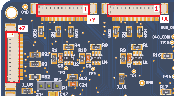
Solar panels connectors
+X, +Y, +Z
| Number |
NAME |
DESCRIPTION |
| 1 |
MAGNETORQUER_A0 |
Magnetorquer Connection 0 |
| 2 |
MAGNETORQUER_A1 |
Magnetorquer Connection 1 |
| 3 |
GND |
Ground |
| 4 |
VCC_5V |
5v Voltage Source |
| 5 |
GYRO_A_CSn |
Gyroscope Chip Select |
| 6 |
SPI1_MOSI |
Serial Command Line |
| 7 |
SUNSEN_A_CATHODE |
Photodiode Cathode |
| 8 |
SUNSEN_A_ANODE |
Photodiode Anode |
| 9 |
SPI1_CLK |
Serial Clock line |
| 10 |
SPI1_MISO |
Serial Read Line |
| 11 |
VCC_3V3 |
3v3 Voltage Source |
| 12 |
TEMP_A_CSn |
Temperature Sensor Chip Select |
JTAG Interface
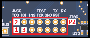 Jtag Interface
P2
| Number |
NAME |
DESCRIPTION |
| 1 |
TDO |
Test Data Output |
| 2 |
VCC_JTAG |
3v3 voltage source |
| 3 |
TDI |
Test Data Input |
| 4 |
|
|
| 5 |
TMS |
Test Mode Select Input |
| 6 |
|
|
| 7 |
TCK |
Test Clock |
| 8 |
TEST |
Test Pin |
| 9 |
GND |
Ground |
| 10 |
|
|
| 11 |
RST |
JTAG Reset |
| 12 |
UART0_TX |
Serial TX |
| 13 |
|
|
| 14 |
UART0_RX |
Serial RX |
Antenna Connectors
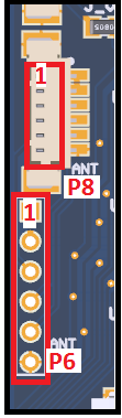 Antenna connectors
P2
| Number |
NAME |
DESCRIPTION |
| 1 |
VCC_3V3_Deployment |
3v3 voltage source |
| 2 |
VCC_3V3_Deployment |
3v3 voltage source |
| 3 |
I2C2_SDA |
Antenna serial data line |
| 4 |
I2C2_SCL |
Antenna Serial clock line |
| 5 |
ANTENNA_DEBUG |
Extra GPIO for antenna microcontroller |
| 6 |
GND |
Ground |
Selection Jumpers

Reset selector (left) and Voltage Selector (Right)
P1
| POSITION |
NAME |
DESCRIPTION |
| 1 |
JRST |
Reset source from JTAG |
| 2 |
WDRST |
Reset source from external watchdog |
P7
| POSITION |
NAME |
DESCRIPTION |
| 1 |
PC104 |
VCC source from PC104 |
| 2 |
JTAG |
VCC source from JTAG |
Debug Connectors
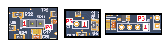 Memories SPI bus(left), Imu's I2C bus(center) and Uart bus with watchdog pulse(right).
P3
| Number |
NAME |
DESCRIPTION |
| 1 |
UART0_TX |
Debug serial TX line |
| 2 |
UART0_RX |
Debug serial RX line |
| 3 |
WDI_EXT |
Watchdog pulse pin |
| 4 |
GND |
Ground |
P4
| Number |
NAME |
DESCRIPTION |
| 1 |
I2C1_SDA |
Imu's Serial data line |
| 2 |
I2C1_SCL |
Imu's Serial clock line |
P5
| Number |
NAME |
DESCRIPTION |
| 1 |
SPI1_CLK |
Memories Serial clock line |
| 2 |
SPI1_MISO |
Memories Read data line |
| 3 |
SPI1_MOSI |
Memoreis Command data line |